Thick film substrates are ceramic-based, hard, and with little dimensional changes. They have excellent resistance to heat, solvents, and wear, and are used for a wide range of uses, such as vehicles, high frequency parts, and industry.
Since we began manufacturing in 1983, we at Miyoshi Electronics and Synergy Technica have actively strived to support everything from pattern design and circuit printing to resistance trimming, as well as to respond to environmental problems and quick prototyping, things that have been required in recent product development. We aim for steady delivery and reliable quality for our customers.
Example of products

Use for Vehicles

General Industrial Use

High Frequency Use
")
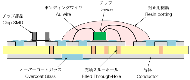
Cu Substrate (General Industrial Use)
[Features]
- Established a quick system through single-process production from design to shipping
- We have pattern designing and pre-press operations in-house, so we can begin manufacturing quickly.
- We have a laser scriber in-house, so we can quickly handle substrates with unusual shapes or through-holes.
Standard working days
- Prototype: Shipped on 7th day of actual operation (For general products where single-side printing and printing work has 5 processes and trimming is done after design approval)
- Mass production product: Shipped on 20th day of actual operation (For general products. Mold substrates require a separate 5 to 9 weeks.)
- Market results
- Since we began production in 1983, we have sold a total of approximately 700 million products on the market.
- We have delivered results for a broad range of uses, primarily for vehicles.
- We use substrates (106 mm x 106mm) as our standard, and depending on conditions, we can handle a maximum of up to 120 mm x 106 mm.
- Establishment of a quality assurance system
- We have acquired ISO9001.
- We are fully equipped with a clean room of the post-semiconductor work grade (10 k to 500 k / 10 km2.) We perform measures to prevent foreign objects, static electricity, and humidity, and to control temperature, thus arranging our stable development system.
- Our in-house, full-process production allows for low cost. Please contact us to request a quote.
- We offer technical support for heat release, high density, and more.
[Uses]
- For vehicles: Ignition control circuits, sensors (pressure, acceleration), fuel tank gauges, etc.
- For high frequency use: power amp circuits for various wireless devices
- For industrial use: power circuits, charging circuits, inverter circuits, sliding resistance, etc.